Researchers say they’ve hacked together nanoscale 3D printing and metal plating to make ultra tiny, high performance RF gadgets.
A newly published study alleges a radical twist in how high frequency tech could be made using nanoscale 3D printing to sidestep the headaches of traditional manufacturing.
The paper, authored by researchers at Bilkent University and Nanyang Technological University, shows off a method that apparently lasers intricate tiny trenches with two photon polymerization, then stuffs them full of copper. The supposed result? RF resonators with freakishly precise tuning (4 6 GHz) and a 1 4 aspect ratio all crammed into a space nearly half the size of usual parts.
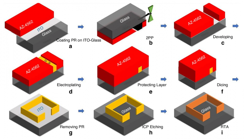
Fabrication process flow. The developed methodology involves the following steps: (a) spin-coating AZ-4562 positive photoresist onto ITO-coated glass, (b) positioning the substrate on the 3D printing system’s sample holder and exposing it to light to define the desired pattern, (c) developing the exposed photoresist regions, (d) depositing a thick copper film over the ITO seed layer following the patterned lines, (e) applying a protective layer via spin-coating, (f) dicing the substrate into smaller segments, (g) stripping away the photoresist, (h) dry etching the ITO seed layer using ICP, and (i) performing thermal annealing to enhance the copper structure’s durability. (Photo Credit: Microsystems & Nanoengineering)
Details are thin on how exactly they pulled it off, but the team claims their hybrid 3D printing and plating trick avoids the usual pitfalls of lithography, like wonky sidewalls or material limits. They even report a sixfold boost in performance metrics (those “Q factor” things engineers love).
“This might bridge 3D printing and functional RF devices,” said Prof. Hilmi Volkan Demir in the paper, carefully not overpromising. The implied upside? Tiny 5G gear, medical sensors, or even IoT gadgets could get way smaller and smarter.
Also read: Amolen Launches Glow-in-the-Dark and Transparent TPU Filaments
Of course, it’s all still lab bound for now. But if the hype holds, this could potentially dethrone decades old lithography for good assuming the tech scales beyond a university basement.